BY HARRY KAO, YOMURA TECHNOLOGIES INC.
In-mold decorating (IMD/IML) also known as film insert molding, the latter being a better description for none decorative parts. This process is sometimes referred to as In-Mold Label, it is a similar process that is primarily used to decorate containers, cups, and various vessels. The technique is the process of decorating an injection molded part with a decorated film during the injection process. The label becomes an integral part of the final product, creating a fully decorated item on the visual surface or partially as with a label on a container. In this process, a pre-printed label or decorated film is inserted in the open plastic injection mold and held in place mechanically, electrostatically, in gravity, or vacuum. When the mold is closed, plastic resin is back injected onto the film encapsulating it permanently within the finished part. Before the advent of the IMD, there were two basic options for decorating molded parts, screen printing, and pasting labels on the part. Both of these techniques cannot equal the flexibility and the durability of IMD. The technique allows more imaginative designs that not only enhance decoration but also provide functionality. The technique lends itself readily to smart surfaces, tactile keys, water-resistant products, electronic circuits, and even optical components that can be integrated cost-effectively. The majority of all the films are second-surface printed, printing on the primary surface is less durable. The second surface printing can be a very simple single color to very complex multiple pass patterns that simulate marble surfaces and include functional optical filters. Second surface printing contributes greatly to the durability of the product and is a major factor in the selection of IMD. The part can be passive or active, with traces and electroluminescent surfaces being included on the film, dead front, filers, over mold, and selective electroplating plating are also design options.
The IMD process essentially has 3 steps, 1. Printing, 2. Forming, 3 back injection. An in-mold label typically skips step 2 as the label is flat and pressed against the mold.
Printing - Screen printing is the most common method for printing films, digital and offset, are less common, Digital UV printing is rapidly gaining ground and will fulfill the long promise of being able to have a different graphic on every molded part without any significant increase in cost. Printing has gone far beyond the simple screen-printed graphics that mimic existing label designs, complex patterns that give a fairly good representation of carbon fiber and marble surfaces are now commonly produced. With the new generation of conductive inks, the ability to print 3D electronics a highly desired process, yet too costly to use, will now become commonplace.
Inks- The IMD process requires special inks, those that are not specially formulated will crack, and yellow when processed. They must be flexible and resistant to washout when stretched. The printing is not uniform across the film, it is frequently necessary to print multiple layers at high stretch areas and, where the resin impinges on the film as it exits the gate. The last layer to be printed is the anti-wash coating, depending on the gate location and injection pressure several layers of the anti-wash may be needed to prevent the ink from being removed from the surface of the film. New developments in conductive ink technology will allow them to withstand the rigors of in-mold processing and still maintain their dielectric properties. Touch panels have become the preferred method of data input to a device and the level of integration will grow with the improvement in the printing of IMD films. Two more steps are required after the graphics are printed, an anti-wash layer is added to help prevent the inks being removed during the injection process. The final layer to be printed is an adhesion promoter, the injected resin in most cases will not naturally form a bond to the printed film. Bonding is critically important as delamination is possible over a period of time if the film is exposed to thermal cycling or contact. The adhesives that are used for this application are thermally activated and require sufficient thermal energy for the adhesive to reach the glass transition temperature. Some experimentation with a part and the adhesive bond is necessary to ensure that the bonding is satisfactory. Mold temperature, dwell time, and injection material temperature play a critical role in ensuring that a satisfactory bond is made.
Films – There are a number of film choices depending on the particular application the product is being designed for.
PA (polyamide) These films have outstanding chemical resistance, high transparency, good mechanical durability, and high heat deflection temperature. They are suitable for use with ABS, PC/ABS, PC, and similar substrate materials.
PC (Polycarbonate) film has very good optical properties, it can be easily thermoformed and has high impact resistance and good heat resistance. Polycarbonate is amorphous and has low chemical resistance.
ABS ( Acrylonitrile butadiene styrene) These films have very good impact strength and they are naturally translucent, they offer a good price-performance ratio, also like PC they have low chemical resistance.
PP ( Polypropylene) They have a great price-performance ratio and outstanding chemical resistance. They are used most frequently in the IML labeling of containers.
PMMA( Polymethylmethacrylate) Has excellent scratch resistance superior to PA and PC when uncoated. It is highly transparent and suitable for optical applications when compared to PC and PA the level of mechanical performance is lower.
PET(Polyester) Has excellent thermal stability, good mechanical properties, high strength, good dimensional stability, and optical clarity. These films are the most used in high-volume consumer products.
Surface treatments on films such as hard coating, anti-glare, anti-fog, satin, and matt finish are available from the suppliers. Care must be taken to avoid sharp edges when designing a part that will use hard-coated film. Hardcoat tends to crack when formed around a small radius, the harder the coat the more generous a radius is required.
Thermoforming- The printed film is then formed typically for the IMD process by pressure thermal forming. A printed sheet is heated and then forced down into a female mold by evacuating the air from it. The material then takes the shape of the mold allowing greater detail to be formed in the part than the traditional vacuum forming. The forming process causes a stretch in the material which can result in deformed or mislocated graphics. To understand the amount of stretch that the film is undergoing, a label printed with a grid pattern is processed. The variations in the grid pattern after processing can readily be seen. This allows the graphic designer to adjust the graphic that could be affected by the stretch. The depth of draw is limited by the part configuration and apparently by the processing ability of the molder with a good processor draw depths of 25mm are possible. Inks are also a factor in the amount of deformation that can be tolerated in the thermal forming process. Modern UV inks are much more resistant to stretch created by the forming process, they will be subject to changes in color density if pushed beyond their limitations.
Trimming – The formed part needs to be trimmed, this is done prior to insertion in the mold or after the injection phase. The trimming cannot be done accurately with a steel rule die, a high-quality match plate tool must be created to accurately trim the film. For high-volume production, the film may be fed into the thermal forming station in role form and post-trimmed. In some applications, the formed shape can be accomplished by a cold-forming process in much the same way a drawn stamped metal part is produced. The entire process of printing the role, stamping, injecting, and trimming is fully automated. The IMD process is becoming more automated with batch printing, auto trim, and back-injected being undertaken by robotics. The process should always take place in clean rooms, dirt on the film or in the mold can cause significant yield loss.
Secondary operations.
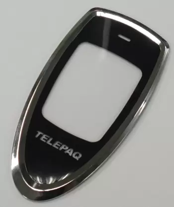
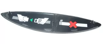
Post process operations such as over-molding, selective plating, and printing are easily accomplished. Below are Figure 1,2 and 3. Here is a short description of the process that achieves the results as shown

Fig 1 Is a Bezel for a handphone. At first look, it appears to be a relatively simple part to manufacture. The first process is the IMD Label containing the window and the black background, the material selected for the part is Polycarbonate. The label is then inserted into the mold and over-molded with platable ABS, this is the bright rim in the picture. The process of plating ABS is well known. To plate the ABS its surface must be modified with an etching solution. The etching solution is based up chromic acid and will not etch the Polycarbonate. After etching the surface is then activated or primed with a solution containing tin and palladium salts. The surface of the ABS is then coated with nickel or copper. The final step is electroplating using conventional technology. As the PC was not etched it cannot be plated, this in short is the selective plating process.

Fig 2 The image below is a familiar sign to anyone who has traveled by on an airliner. This is the view from the back, the front side is not shown, it is a dead front panel, and the graphics cannot be seen until the sign is illuminated. The front surface is screen printed in a color that matches the surrounding structure and is translucent. The reverse side is a screen printed with translucent graphics. The black background is printed to prevent light transmission. The label is then back injected with clear Polycarbonate to form the finished part.
IMD once an expensive option for product designers has become a very effective and reasonably priced option. The quality is far superior to that of a molded part that is decorated by screen or pad printing and/or has an adhesive label attached to a flat surface. The process can now provide complex options for the designer to consider. They can add a high level of functionality, complex graphics, optical, mechanical, and electrical functions in a self-contained assembly. Improvements in films, inks, adhesives, and electronics are continuing to be made. The future for the IMD process is bright with the introduction of smart surface technology.
